60 Second Timer - May 2015
Project Overview
|
This project's goal was to create a 60 second timer. The counter counted from zero to fifty nine. The counter used a '163 synchronous counter for the ones place and a series of three J/K flip flop asynchronous counters for the tens place. The circuit had two inputs- the clock and the reset. The reset made both the ones and tens place go to zero, then start counting again. The clock itself was only connected to the synchronous counter. The output of this counter served as a clock for the J/K flip flops.
|
PLD Circuit

This circuit consisted of a 74LS163 synchronous counter for the ones digit of the count and three J/K flip flops for the tens place. A clock controlled the count for the ones place and the output of the '163 counter served as the clock for the tens place, so that when the count reached a 1001, or nine, the tens place would advance by one. The circuit loops so that once the number 59 is reached, the count starts over at 0. A reset button is also included. It's connected to the load for both the ones and tens place. The circuit is then put through a multiplexer so that both digits can be displayed on the breadboard.
Conclusion
Difference Between Synchronous and Asynchronous Circuits:
Asynchronous circuits are asynchronous because all the flip flops do not sync to the same clock. They link through each other, with each flip flop serving as a clock for the next one. This leads to the Ripple Effect, where the last flip flop in the chain lags slightly behind the ones before it because the clock signal must travel through multiple flip flops to reach it. Synchronous counters, however, don't have this problem. All the flip flops connect to the same clock, eliminating the Ripple Effect found in asynchronous counters. They are also much quicker than asynchronous counters. However, they require more logic to build.
Difference between '163 and '193:
Both 74LS163 and 74LS193 are MSI synchronous counters, but they have some major differences. '163 counters are unique in that what number is caught by the NAND gate is the last number shown. With '193 and all other counters, the reset number is the last number of the count plus one. While both '163 and '193 can start with any number up to fifteen, '163 counters can only count up. '193 can count up or down.
Process I Used to Create my Design:
In building my circuit, I decided to begin in PLD mode, as I did not want to design the circuit twice. I started with the ones place and the synchronous counter. The counter used was a '163, but in PLD mode was called "CNTR_4BIN_S". I connected all four inputs to DIGITAL_LOW (the DGRD in PLD mode), so the count would start at zero. I connected the ENP and ENT inputs to DIGITAL_HIGH (the VCC in PLD mode). I inserted the DIGITAL_CLOCK and connected it to the CLK input. I then set up four probes to the right of the counter so that I would be able to view the output. I connected the outputs each to a different probe so that, from left to right, they are connected to D, then C, then B, then A. This puts them in order from Most to Least Significant Bit, and makes the binary number readable. Next, I inserted a four-input NAND gate. This NAND gate would determine what the reset would be for the counter. Because I wanted it to count from zero to nine, I connected the NAND gate directly to the outputs of D and A and added two inverters with which to connect through to B and C. Because '163 is unique in that a "count+1" is not needed for the load, a nine that is caught as the last number will still be displayed. I connected the output of the NAND gate to the LOAD input on the '163 counter.
Next, I inserted three J/K flip flops into my design. These are called "FF_JK_PSCLR_CO" in PLD mode. All three flip flops had multiple inputs that connected to DIGITAL_HIGH- all the Presets, J's, and K's. The NotQ of the first flip flop connected to the CLK of the second counter and the NotQ of the second counter connected to the CLK. I inserted three probes with which to monitor the outputs, then connected the Q outputs to the probes so that the far right flip flop connected to the leftmost probe, the second probe to the second flip flop, and the left flip flop to the probe furthest to the right. This put the probes in order from MSB to LSB. After setting up the outputs, I had to make the reset. I inserted a three-input NAND Gate and connected it to the Q of the third and second flip flops and the NotQ of the first flip flop. This would catch a six, making the count go from zero to five, then reset. I connected the output of the NAND gate to a two-input AND gate. This served as a place for the reset button to connect to later. Then, I connected the output of the AND gate to the CLR of each of the three flip flops.
For the reset, I added an INTERACTIVE_DIGITAL_CONSTANT. I connected this to the CLR of the '163 counter and the AND gate that connected to the clear on the flip flops.
After the design was complete, I connected it to a multiplexer. I added two input pins, 14 and 10, that would serve as inputs when I breadboarded. The clock always connects to pin 14. I chose pin 10 to connect to the reset button.
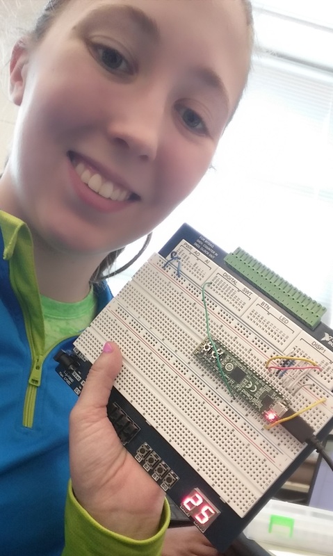
After designing my circuit and testing that it worked, I built it on the board. I connected the clock to pin 14, a switch to pin 10, powered pin 24 and grounded pin 25, connected pins 26-32 to G through A on the seven-segment display, and the ones display to pin 33 and the tens display to pin 34. After transferring the program to the board and testing it, it worked as expected.
My Design versus my Classmates' Designs:
My design was similar to the designs of the majority of my classmates. Chase's was much similar than mine was.
Asynchronous circuits are asynchronous because all the flip flops do not sync to the same clock. They link through each other, with each flip flop serving as a clock for the next one. This leads to the Ripple Effect, where the last flip flop in the chain lags slightly behind the ones before it because the clock signal must travel through multiple flip flops to reach it. Synchronous counters, however, don't have this problem. All the flip flops connect to the same clock, eliminating the Ripple Effect found in asynchronous counters. They are also much quicker than asynchronous counters. However, they require more logic to build.
Difference between '163 and '193:
Both 74LS163 and 74LS193 are MSI synchronous counters, but they have some major differences. '163 counters are unique in that what number is caught by the NAND gate is the last number shown. With '193 and all other counters, the reset number is the last number of the count plus one. While both '163 and '193 can start with any number up to fifteen, '163 counters can only count up. '193 can count up or down.
Process I Used to Create my Design:
In building my circuit, I decided to begin in PLD mode, as I did not want to design the circuit twice. I started with the ones place and the synchronous counter. The counter used was a '163, but in PLD mode was called "CNTR_4BIN_S". I connected all four inputs to DIGITAL_LOW (the DGRD in PLD mode), so the count would start at zero. I connected the ENP and ENT inputs to DIGITAL_HIGH (the VCC in PLD mode). I inserted the DIGITAL_CLOCK and connected it to the CLK input. I then set up four probes to the right of the counter so that I would be able to view the output. I connected the outputs each to a different probe so that, from left to right, they are connected to D, then C, then B, then A. This puts them in order from Most to Least Significant Bit, and makes the binary number readable. Next, I inserted a four-input NAND gate. This NAND gate would determine what the reset would be for the counter. Because I wanted it to count from zero to nine, I connected the NAND gate directly to the outputs of D and A and added two inverters with which to connect through to B and C. Because '163 is unique in that a "count+1" is not needed for the load, a nine that is caught as the last number will still be displayed. I connected the output of the NAND gate to the LOAD input on the '163 counter.
Next, I inserted three J/K flip flops into my design. These are called "FF_JK_PSCLR_CO" in PLD mode. All three flip flops had multiple inputs that connected to DIGITAL_HIGH- all the Presets, J's, and K's. The NotQ of the first flip flop connected to the CLK of the second counter and the NotQ of the second counter connected to the CLK. I inserted three probes with which to monitor the outputs, then connected the Q outputs to the probes so that the far right flip flop connected to the leftmost probe, the second probe to the second flip flop, and the left flip flop to the probe furthest to the right. This put the probes in order from MSB to LSB. After setting up the outputs, I had to make the reset. I inserted a three-input NAND Gate and connected it to the Q of the third and second flip flops and the NotQ of the first flip flop. This would catch a six, making the count go from zero to five, then reset. I connected the output of the NAND gate to a two-input AND gate. This served as a place for the reset button to connect to later. Then, I connected the output of the AND gate to the CLR of each of the three flip flops.
For the reset, I added an INTERACTIVE_DIGITAL_CONSTANT. I connected this to the CLR of the '163 counter and the AND gate that connected to the clear on the flip flops.
After the design was complete, I connected it to a multiplexer. I added two input pins, 14 and 10, that would serve as inputs when I breadboarded. The clock always connects to pin 14. I chose pin 10 to connect to the reset button.
After designing my circuit and testing that it worked, I built it on the board. I connected the clock to pin 14, a switch to pin 10, powered pin 24 and grounded pin 25, connected pins 26-32 to G through A on the seven-segment display, and the ones display to pin 33 and the tens display to pin 34. After transferring the program to the board and testing it, it worked as expected.
My Design versus my Classmates' Designs:
My design was similar to the designs of the majority of my classmates. Chase's was much similar than mine was.
